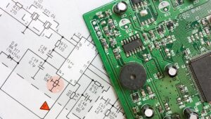
Implementing an emission and immunity compliant PCB design controls the interference between circuits, and is important for the proper function and durability of the circuit. By integrating low-EMI principles into the PCB design process, manufacturers can achieve reliable, high-quality products that meet industry requirements, such as those assessed during EMI & EMC testing services and FCC compliance testing. Nine fundamental steps for low-EMI PCB design are described below with the inclusion of contemporary compliance strategy.
Step 1: Optimize PCB Layout Design
Good and carefully planned placement of PCB layout is therefore a key starting point to reducing EMI or in fact controlling emanation. This means minimising the area of the loops that are in the signal path and which act as antennas for EMI. Key considerations include:
- High-speed components should be positioned near a connector.
- Reducing trace lengths that can cause radiation and crosstalk.
- Shielding by ground planes to protect the designated signals and also give a low resistance return path.
An optimized layout streamlines compliance during EMI EMC testing services, ensuring products meet regulatory standards.
Step 2: Implement Grounding Techniques
The case with grounding is that they are very effective for EMI control when properly installed. Techniques include:
- Dedicated Ground Planes: Using separate planes for power and signal ground reduces noise.
- Stitching Vias: Ensuring multiple connections between ground planes improves current return paths.
- Short Ground Loops: Keeping loops minimal reduces susceptibility to interference.
These practices improve signal integrity, easing wireless device testing and RF testing services.
Step 3: Use Decoupling Capacitors
High frequency noise is reduced by the decoupling capacitors, through the establishment of power supply levels. Proper placement and selection are crucial:
- Capacitors should be placed near the power pin of integrated circuits (ICs).
- For high-frequency decoupling you should use capacitors with low ESR known as Low Equivalent Series Resistance capacitors.
This step supports smoother performance during compliance management solutions evaluations.
Step 4: Minimize Crosstalk
Crosstalk is a condition where signals in different traces overlap each other. Techniques to reduce crosstalk include:
About the usefulness of the proposed method, there are the following opinions:
- LIS: Adhering to the differential pair routing for high speed signals.
- Working with practical planes to provide separation between layers, and the like.
This proactive approach enhances results during RF testing services and ensures robust designs.
Step 5: Shield High-Frequency Components
According to the research, electromagnetic interference can be tremendously minimized through the practice of shielding. Key actions include:
- Positioning shielding cans on areas that produce noise.
- Transmission of fast signals from one internal PCB layer to another.
- Including the Faraday cages for sections that are sensitive.
These measures simplify wireless compliance testing and reduce the chances of FCC compliance testing failure.
Step 6: Utilize Controlled Impedance
Controlled impedance design is the practice aimed at reducing signal reflection and loss. Best practices include:
- The ability to match trace impedance with the source and load.
- It was found that impedance of the modeled system can be verified using simulation tools.
- Adding the right type of termination resistors so that actual reflections are avoided.
By achieving consistent impedance, products are more likely to pass EMI EMC testing services on the first attempt.
Step 7: Implement Power Integrity Practices
The conditions under which electrical and mechanical interfaces remain clean and supply power cleanly will reduce the sources of EMI. Best practices include:
- Doing it by employing a low inductance power distribution network (PDNs).
- It also involves putting bypass capacitors appropriately.
- Using ferrite beads for noise, primarily at high frequency, reduction.
These actions align with compliance management solutions for regulatory testing.
Step 8: Perform Pre-Compliance Testing
Before they are sent for the official certification, a pre-compliance test is necessary to help in finding the Elmi problem areas. Tools and services include:
- Spectrometers for emission.
- Near-field probes for accurate identification of the interference locations.
- Collaboration with compliance software solutions to automate reporting.
Proactive pre-compliance testing can save time and costs during wireless product certification
Step 9: Follow Industry Standards and Guidelines
Adhering to standards from all over the world means compatibility; the process of certification will also be easier. Key references include:
- FCC Guidelines: For devices entering the U.S. market.
- ISO/IEC Standards: Covering electromagnetic compatibility globally.
- Industry-Specific Norms: For medical, automotive, or telecom sectors.
Compliance with these frameworks facilitates seamless wireless compliance testing and enhances product reliability.
Conclusion
Low-EMI PCB design is a complex attainment and complication of design strategies and the compliance of methodologies. By optimizing layout, grounding, shielding, and power distribution while adhering to industry standards, manufacturers can ensure successful EMI & EMC testing services outcomes. Pre-compliance testing and collaboration with compliance management solutions further streamline certification, enabling market-ready products that meet regulatory demands.
Partnering with experts in RF testing services, FCC compliance testing, and wireless product certification ensures your designs are ready for global success. These steps must be warmly welcomed in order to create solid, compliant designs that will wow the user.
